![]() October 10, 2023
October 10, 2023
Visit to Nanoscience Research Laboratory

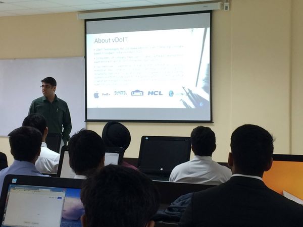
Students from Bachelors of Science and Master of Science of the Physics and Chemistry programs were given with an opportunity to visit Nanoscience Research Laboratory of Miranda House, University of Delhi on 10 October 2023.
They experienced the working in the Clean Room Laboratory - Material Processing and Device Fabrication, where the working and principle of sophisticated instruments such as photolithography, RF Magnetron sputtering, instruments of physical vapor deposition and thin layer deposition techniques were explained and the fabricated samples were exhibited.
The students were also made familiarized with sol-gel, chemical vapor deposition techniques, working of high temperature muffle furnace and gas sensing techniques using fabricated materials. The electrical properties of materials using piezoelectric, pyroelectric, thermoelectric and triboelectric techniques were also exhibited and explained.
Our Blogs Similar Blogs
 Html->link($this->Html->image('blogs/'.$img), ['controller'=>'medias','action'=>'blogdetail',$similarn['posturl']], array('escape' => false)); ?>
 Html->link($this->Html->image('blogs/'.$img), ['controller'=>'medias','action'=>'blogdetail',$similarn['posturl']], array('escape' => false)); ?>
 Html->link($this->Html->image('blogs/'.$img), ['controller'=>'medias','action'=>'blogdetail',$similarn['posturl']], array('escape' => false)); ?>
 Html->link($this->Html->image('blogs/'.$img), ['controller'=>'medias','action'=>'blogdetail',$similarn['posturl']], array('escape' => false)); ?>
Connect with UsTalk to our Admissions Counsellor
+91 9910000062